We believe the photon is the key to building future devices for quantum technology. Whether used for quantum imaging, sensing, carrying information in a quantum computer, or for linking nodes in the quantum internet, it will be at the centre of all future quantum technologies.
Using our expertise in constructing semiconductor devices that create and manipulate photons, we perform research that bridges between engineering, physics, materials and technology.

Practical quantum light sources
We research materials that emit quantum light at room temperature. These materials are all wide-band-gap semiconductors that host a combination of impurities and vacancies that can give the crystals colour, these are known as “colour centres”.
The most famous example is the Nitrogen Vacancy (NV) centre in diamond. It shows great promise as a field sensor owing to the presence of a spin-triplet in the ground state, which can be optically pumped and microwave driven. We are also working on colour centres in materials such as aluminium nitride, gallium nitride and boron nitride that have recently joined the elite selection of materials that emit quantum light at room temperature. Their presence in commercially-mass-produced materials and 2D layers opens the possibility of new device designs and novel applications in quantum technology.
Research papers
Quantum sensing with photons and spin
Quantum technology can be harnessed to build sensors that are better at measuring the world around us. Semiconductor devices can miniaturise this functionality to create compact, robust and precise sensors, electric fields, magnetic fields, strain, refractive index and other properties.
Many of these technologies result from the parameter we are trying to measure affecting a resonance in some quantum system. This could be the frequency at which a spin rotates in a diamond crystal being changed by a magnetic field, or the energy at which an optical cavity resonates as a fluid passes over it. Working with collaborators we have developed the underpinning technology for these sensors in several different wide-band-gap semiconductors.
Research papers
Quantum technologies in diamond enabled by laser processing
Coherence protection of spin qubits in hexagonal boron nitride
Advanced light sources for quantum optics
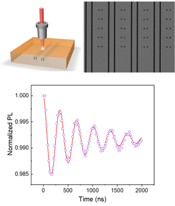
Self-assembled quantum dots are among the most advanced single photon sources available, with decades of research into their development. They can generate photons with exceptional purity and efficiency when integrated into monolithic cavities, and operated at cryogenic temperatures.
We are working as part of the UK National Hub in Quantum Computing and Simulation to refine these sources for optical quantum information processing. Semiconductor material is sourced from the National Epitaxy Facility in Sheffield, etched in Cardiff’s cleanroom, and assessed in our labs. Collaborations with other groups drive this project, most strongly with the National Physical Laboratory who are interested in redefining the SI unit of light using these exceptional photon sources.
Research papers
Electrical control of semiconductor quantum dot single photon sources
Two-Photon Interference of Single Photons from Dissimilar Sources
A quantum dot as a source of time-bin entangled multi-photon states

Semiconductor processing technology
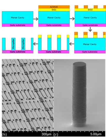
Our group works at Cardiff University’s Institute for Compound Semiconductors Cleanroom, which is a state-of-the-art research hub opened in 2023 to facilitate the manufacture of devices for research and industry. This 1,500 sqm facility includes a large array of new lithography, etch, deposition and fabrication technologies supported by experienced technicians. We use this unique facility to support our research into novel processing technologies, such as Faraday cage etching of gallium nitride and maskless projection lithography of high quality single photon sources for the UK’s National Quantum Computing and Simulation Hub.
New starters are encouraged to undergo cleanroom training, to acquire a sought after skill in industry, and gain independent control over the direction of their project.
Research papers
Direct-write projection lithography of quantum dot micropillar single photon sources
Faraday-cage-assisted etching of suspended gallium nitride nanostructures
Nanophotonic simulations
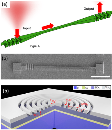
The group has delivered several projects in the design of novel nanophotonic devices. The relatively high refractive indices of semiconductors means this work is required to optimise coupling of photons into, and out of, the crystal.
Our focus is always on devices we can manufacture in Cardiff’s cleanroom, but in many cases the simulations are scientifically interesting in themselves. We use commercial software and access to Cardiff University’s Supercomputer (ARCCA) to simulate devices using Finite-difference time domain methods, often in collaboration with colleagues in the School of Physics and Astronomy. In the figure we show (a) an optimised design of grating coupler etched into a triangular gallium nitride waveguide, (b) an electron microscope image of a real device of this type and (c) a Bullseye Bragg grating to enhance the intensity of quantum light from a monolayer-thick semiconductor.
Research papers
Bullseye dielectric cavities for photon collection from a surface-mounted quantum-light-emitter
Design of free-space couplers for suspended triangular nano-beam waveguides
Topological insulator laser using valley-Hall photonic crystals
Photonic integrated circuit microfluidic sensing
Photonic integrated circuits can also be used for sensing. We have been working with Welsh Water, and Wave Photonics on development of photonic integrated circuits sensors for contaminants in water.
We have been working with CORNERSTONE – the EPSRC funded Silicon Photonics foundry to develop scalable Silicon Nitride devices which are functionalised in collaboration with our colleague in the school of Biosciences to selectively sense water contaminants such as heavy metals. In the figure we show a) an electron microscope image of a silicon nitride microring resonator sensor which can interact with fluids in a microfluidic channel etched into the device.
